Cable Compensation of a Primary-Side-Regulation Power Supply
Abstract
Cable compensation has been used to compensate the voltage drop due to cable impedance for providing a regulated charging voltage in battery charger applications. This application note uses a novel cable compensation method, which called cable minus compensation, as an example to describe the concept and design criteria for the cable compensation of a PSR flyback converter. The analytic results are also verified by the simulation results.
A flyback converter with primary side regulation (PSR) is widely used in off-line battery charger applications due to low cost and simplicity. In a PSR, the output voltage is indirectly sensed through the auxiliary winding, and good regulation can be achieved with the precise detection circuit. However, in such applications, there is a long cable connected between the adaptor output and the electronic devices, such as cell phone, tablet, and so on. If the output voltage is perfectly regulated, there is a voltage drop at the cable end while the output current flows through the cable impedance. The decreasing charging voltage will extend the charging time and even violate the regulation specification especially for the situation under low output voltage and high output current application. This phenomenon can be illustrated in Figure 1.
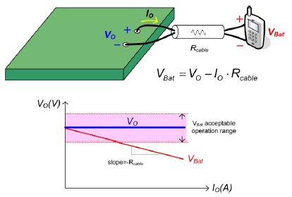
Figure 1. The Voltage Drop Due to Cable Impedance
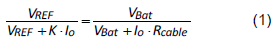
Cable compensation is used to compensate the cable voltage drop by linearly increasing the output voltage VO with the output current IO. Figure 2 shows these two methods used to realize cable compensation. One is called cable plus compensation, which adds the compensation signal K∙IO to the reference voltage VREF and feeds into the non-inverting terminal of the error amplifier. The desired compensation voltage can be accurately reflected on the increment of the reference voltage through the compensation signal K∙ IO, and the DC gain K can be obtained from (1). The other is called cable minus compensation. This scheme subtracts the compensation signal K∙ IO from the feedback voltage VFB and pass through Zi into the inverting terminal of the error amplifier.
However, the output current cannot directly be sensed in PSR applications. Figure 3 shows the circuit diagram of a PSR flyback converter with cable minus compensation. In the diagram, the compensation signal is injected from the signal VCS in the primary side through a buffer with compensator DC gain KCC and a low pass filter (LPF) to indirectly estimate the output current. Current sensing resistor RS is used to transfer the voltage signal VCS from the primary side current signal IP. If the cutoff frequency of LPF or the DC gain KCC is not properly designed, the output voltage may incur oscillation problem and the circuit will be unstable. Therefore, a comprehensive small signal analysis will be provided in the following section for the cable compensator and the feedback control design of a PSR flyback converter.
Figure 2. Cable Compensation Implementation Methods with (A) Cable Plus Compensation, and (B) Cable Minus Compensation.
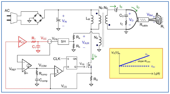
Figure 3. Circuit Diagram of a PSR Flyback Converter with Cable Minus Compensation.
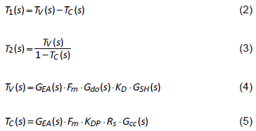
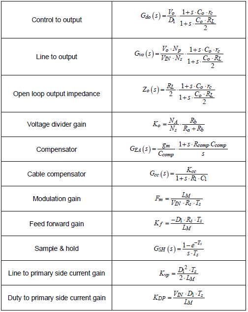
Figure 4 shows the control block diagram of a PSR flyback converter with cable minus compensation. Table I summaries the transfer functions used in the control block diagram. From the control block diagram as shown in Figure 4, there are two loop gains T1 and T2, which are respectively measured at point A and point B, can be found in the feedback loop. They can be expressed as (2) and (3) with reference to the voltage loop gain TV and the current loop gain TC. TV and TC can be respectively represented as (4) and (5).
When the cable compensation involves in the feedback loop, it is surprisingly found that the loop gain T2 is a positive feedback loop which the output voltage VO has the same phase with the error amplifier output VCOM. The positive feedback loop tends to let system become unstable. However, the system stability can be achieved by imposing a negative feedback loop. The loop gain T1 provides a negative feedback loop and is used to determine the system stability. The stability criterion needs to be fulfilled by letting the loop gain T1 cross 0 dB with –20 dB/decade slope and have adequate phase margin.
Although the loop gain T2 is not used to determine the system stability, it influences the output impedance. From the control block diagram shown in Figure 4, the output impedance can be obtained as (6). Not like the traditional thinking, the output impedance is designed to be as low as possible for achieving good load regulation. In order to provide proper cable compensation, the output impedance is expected to have a negative impedance to mitigate the cable impedance. If the output impedance can be designed as –Rcable, the cable impedance seems to be cancelled and the charging voltage is regulated without voltage drop.

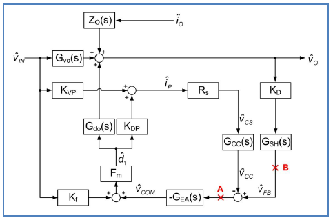
Figure 4. Control Block Diagram of a PSR Flyback Converter with Cable Minus Compensation.
Table I : Transfer Functions of a PSR Flyback with Cable Compensation.
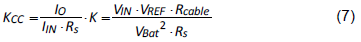
Cable compensation can be effectively accomplished by subtracting the compensation signal K∙IO from the feedback voltage VFB. However, in PSR applications, the average signal of VCS with a DC gain KCC is fed as the compensation signal instead. In order to achieve proper cable compensation, the DC gain KCC can be obtained from (7). Lower KCC leads to the output voltage under-compensated, but higher KCC causes the output voltage over-compensated and may incur unstable problem.
LPF is used to obtain the average value of KCC∙ VCS by filtering out the high switching frequency part. When the cutoff frequency is lower, the high frequency signal of KCC∙VCS can be effectively attenuated and the system tends to be more stable. However, it will pay more area with larger passive components and become unattractive for the practical integrated circuit design. Therefore, the cutoff frequency is a trade-off design between the component size and the system performance.
The goal of the compensator design is to find proper compensator gain GEA such that the loop gain T1 can meet the bandwidth requirement with specified phase margin. The compensator can be designed according to (8) and (9). When the magnitude of Gdo∙KD is larger than KDP∙RS∙GCC, Gd can be approximated to Gdo∙KD, which has one pole and one zero at the left hand plane. The compensator can be easily designed like traditional voltage mode control without considering the current loop TC. It provides one pole at origin and one compensation zero to cancel the system’s pole to make the loop gain T1 stable by crossing 0 dB with –20 dB/decade slope.
However, when the magnitude of KDP∙RS∙GCC approaches Gdo∙KD, there are two poles and two zeros existing in Gd as shown in (9). As the cutoff frequency of LPF gradually increases, the magnitude of KDP∙RS∙GCC starts to be larger than Gdo∙KD during some frequency range as shown in figure 5. When this situation happens, the two left-half-plane zeros of Gd move to the right-half-plane and the system tends to become unstable. Therefore, the compensator can be designed from (8) by neglecting KDP∙RS∙GCC first. The cutoff frequency of LPF can then be design to let KDP∙RS∙GCC be always less than Gdo∙KD for system stability.

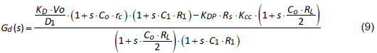
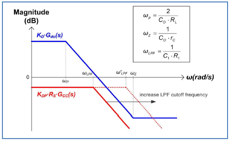
Figure 5. The Plots of KDP∙RS∙GCC and Gdo∙KD.
Simulation is used to verify the analytic results, and the parameters are listed as follows. VIN = 156V, VBat = 5V, IO = 1A, LM = 1.5mH, CO = 1mF, rC = 20mΩ, RS = 4.5Ω, Rcable = 240mΩ, NP : NS : NA = 15:1:1.4, fS = 50kHz, VREF = 1.2V, gm = 100μA/V, Rcomp = 215kΩ, Ccomp = 12nF, Ra = 29kΩ, Rb = 6kΩ, R1 = 100kΩ, C1 = 5nF, and KCC = 400m. Figure 6 shows the simulation waveforms with and without cable compensation, and cable compensation provides proper voltage drop compensation under different load conditions. Figure 7 and figure 8 respectively show the loop gains T1 and T2. The simulation results are well matched with the calculation results. The system bandwidth and phase margin can be determined form the loop gain T1, and it can be observed that the loop gain T2 is a positive feedback. Figure 9 shows the output impedance. The DC gain of the output impedance is close to Rcable but the phase starts from 180°, which means it can provide negative impedance for effectively cancelling the cable impedance.

Figure 6. Simulation Waveforms with and without Cable Compensation.
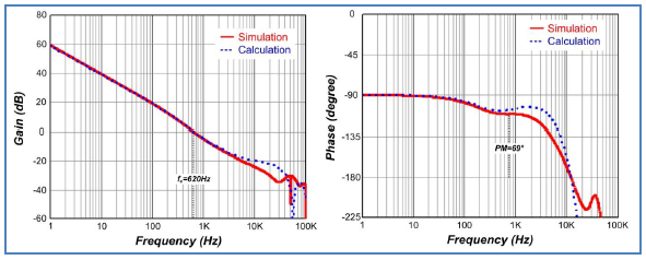
Figure 7. Bode Plots of Loop Gain T1
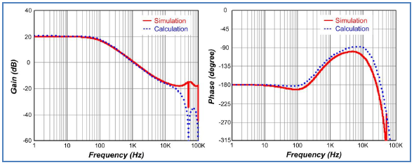
Figure 8. Bode Plots of Loop Gain T2
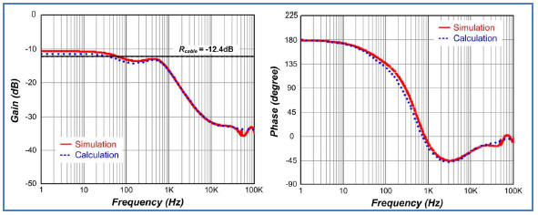
Figure 9. Bode Plots of the Output Impedance.
Figure 10 shows simulation and calculation results with different cutoff frequency of LPF by changing C1. Higher cutoff frequency of LPF incurs unstable problem, and this instability phenomenon can also be predicted according to the loop gain T1 proposed in the previous analytic result. The minimum value of C1 can be determined from the plots of KDP∙RS∙GCC and Gdo∙KD with fixed R1. Figure 11 shows the plots of KDP∙RS∙GCC and Gdo∙KD with different C1 values, and it can be found C1 has to be greater than 3nF for satisfying the condition that KDP∙RS∙GCC is always less than Gdo∙KD. The simulation also confirmed the result with the minimum C1 equals to 4nF.
Figure 12 shows the bandwidth and the phase margin of loop gain T1 with different C1 values. From the figure, it can be found that the system tends to have higher bandwidth and phase margin with larger C1 value. However, when C1 is beyond certain value, the system performance has no significant improvement but extra component size is unnecessarily paid. Therefore, the small signal analysis proposed in this paper provides a useful tool to design the proper cutoff frequency of LPF.
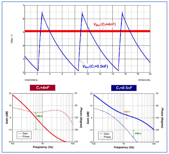
Figure 10. Simulation Waveforms of the Charging Voltage VBat and Calculation Results of Loop Gain T1 with Different C1
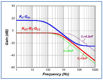
Figure 11. The Plots of KDP∙RS∙GCC and Gdo∙KD with Different C1.

Figure 12. The Bandwidth and the Phase Margin of Loop Gain T1 with Different C1
5. Summary
A PSR flyabck converter with cable minus compensation was proposed to tackle the voltage drop due to the cable impedance in battery charger applications. The small signal model presented in this paper provided a comprehensive tool for small signal analysis and feedback control design to fulfill proper cable compensation. The analytic results were also explained and successfully verified by the simulation results.